Abstract: This article is a supplement to the HFRD-16.0 reference design: 1Gbps to 4.25Gbps active SFP copper Cable Assembly. Explains the use of DS28CZ04 as a serial control interface in active copper cable SFP components. Readers are advised to look up some related reference designs in order to have a deeper understanding of this article.
Overview Fibre Channel, Gigabit Ethernet and InfiniBand ™ networks exchange data at rates higher than 1Gbps. The standard interface of these devices is the SFP (Small Form Pluggable) port, which has the same function as GBIC (Gigabit Interface Converter), but the size is more compact and the density is higher. The active copper cable SFP component can be directly inserted into the SFP port, and the transceiver embedded in the cable Connector can recover and condition the signal so that it can transmit a distance of up to 20 meters at a rate of 4.25Gbps. The Small Pluggable (SFP) Transceiver Multi-Source Agreement (MSA) ¹ defines mechanical (physical dimensions) and electrical interfaces (pin configuration, protocols, etc.), including module specification definitions, interface and data field descriptions. These plug-and-play data formats, also known as SFP serial numbers, are stored in the CMOS EEPROM of the I²C bus interface. DS28CZ04² 4kb I²C / SMBus ™ EEPROM fully meets SFP requirements. Its general-purpose I / O interface can provide additional functions for controlling the MAX3982 copper cable driver or transmitting the status of the MAX3748A receiving signal through the serial port. Circuit diagram 1 gives a simplified schematic of the circuit used at both ends of the cable. The upper left part of the block diagram is the SFP connector, including all signal and pin configurations. The correspondence between pin names and signal functions is shown in Table 1. The DS28CZ04 I²C memory chip is connected to MOD-DEF1, MOD-DEF2 and the power / ground terminal of the transmitter. To ensure the correct SFP slave address, connect address pins A1 and A2 to ground. The write protection (WP) and host reset (MRZ) functions are not used. These two pins are ground (WP) and power supply (MRZ) respectively. PIO2 and PIO3 control the input of U2 (MAX3982³ driver chip), and transmit the data from the SFP connector to the differential input terminal of U2 in the form of AC coupling. The differential output directly drives the cable. The differential output amplitude can be set to one of two levels through the OUTLEV input (controlled by PIO1). For the connection details of other U2 pins, please refer to HFRD-16.0 above. In the figure, the TX disable signal from the SFP connector controls the output of the MAX3982 driver. In the absence of data transmission, this method can turn off the differential output. Another way is to not use the external TX disable signal, but disable the MAX3982 output when no differential input signal is detected. In this case, the LOS output of the MAX3982 can be directly connected to the TX_DISABLE input terminal, and the TX_DISABLE terminal of the MAX3982 is built in. Pull resistance. The third method is to synthesize the above two methods of controlling TX_DISABLE. An additional 2-input OR gate is required, one of which is connected to the TX disable terminal of the SFP connector, and the other is connected to the LOS output of the MAX3982 and passed The 10kΩ pull-up resistor is connected to VCCT. The OR gate output drives the TX_DISABLE input of the MAX3982. The input signal from the cable is fed into U3 (MAX3748A4 receiver) by AC coupling. In U3, the signal is restored to its original amplitude, and the restored signal is then passed to the SFP connector by AC coupling. If the signal from the cable is lost or the amplitude is too small, U3 will send a LOS alarm signal to the SFP connector and the PIO0 port of the DS28CZ04. The LOS of the MAX3748A is an open collector output. A pull-up resistor of 4.7kΩ to 10kΩ is required to connect to the VCCR of the main controller, which is marked as MSA. For the connection method of U3 other pins, please refer to the HDRD-16.0 manual. 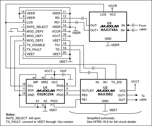 Figure 1. Simplified block diagram of DS28CZ04 for active copper cable SFP components Table 1. SFP Connector Pin Assignment Table 1. SFP Connector Pin Assignment
 | Pin Number | Name | FuncTIon |
| 1 | VEET | Transmitter Ground |
| 2 | TX_FAULT | Transmitter Fault IndicaTIon, acTIve-high; low indicates normal operaTIon |
| 3 | TX_DISABLE | Transmitter Disable, active-high; low indicates normal operation |
| 4 | MOD_DEF2 | Module Definition 2, SDA, I²C data line |
| 5 | MOD_DEF1 | Module Definition 1, SCL, I²C clock line |
| 6 | MOD_DEF0 | Module Definition 0, tied to ground on the board |
| 7 | RATE_SELECT | Optional Input: select between full or reduced receiver bandwidth; low / open indicates reduced bandwidth, high indicates full bandwidth |
| 8 | LOS | Loss of Signal (from receiver chip), active-high; low indicates normal operation |
| 9 | VEER | Receiver Ground |
| 10 | VEER | Receiver Ground |
| 11 | VEER | Receiver Ground |
| 12 | RD- | Inverted Received Data Out (from receiver chip) |
| 13 | RD + | Received Data Out (from receiver chip) |
| 14 | VEER | Receiver Ground |
| 15 | VCCR | Receiver Power, 3.3V ± 5% DC |
| 16 | VCCT | Transmitter Power, 3.3V ± 5% DC |
| 17 | VEET | Transmitter Ground |
| 18 | TD + | Transmit Data In (to transmitter chip) |
| 19 | TD- | Inverted Transmit Data In (to transmitter chip) |
| 20 | VEET | Transmitter Ground |
DS28CZ04 is used as the serial control interface of SFP as shown in the block diagram of Figure 2. The DS28CZ04 consists of a 2-wire serial interface, 4kb EEPROM, and four bidirectional PIOs. connection. DS28CZ04 addresses 512 memory addresses through a memory address and two slave addresses (usually A0h, A2h). 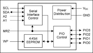 Figure 2. Block diagram of DS28CZ04 DS28CZ04 contains 512 bytes of memory, divided into two sections (low section, high section) in units of 256 bytes (Tables 2A and 2B). The memory image and device addressing comply with the SFF-8472 digital diagnostic address allocation requirements, and the WP can be terminated to VCC to write-protect the entire EEPROM. The PIO pin can be addressed once (single address mode) or independently (multiple address mode). Direct addressing PIO can quickly generate data and sample data. DS28CZ04 includes several EEPROM registers for customers to choose the device to power on in SFF mode or define the following power-on default conditions: the output status of each PIO (high and low, input / output mode), the data direction of each PIO (Input, output), the output type of each PIO (push-pull, open-drain) The read bit of each PIO is inverted (true and false). Once powered up, you can rewrite the PIO setting through the SRAM register without Will affect the power-on default value. Figure 3 shows the simplified schematic of the PIO. The flip-flop can be addressed through the PIO R / W addressing register, memory addresses 7Ah and 7Bh (device address is A0h). At power-up or reset, the flip-flop is initialized according to the data stored in 76h and 77h (device address is A0h). When PIO is set as input, the PIO output is tri-stated (high impedance). When PIO is set to output, the input end of PIO is the result of the inverse XOR of the corresponding read bit. Table 2A. Memory map (device address = A0h)
 | Address | Type | Access | Description |
| 00h to 74h | EEPROM | R / W | User memory |
| 75h | EEPROM | R / W | Special function / user memory; controls whether device powers-up into SFF Mode |
| 76h | EEPROM | R / W | Power-on default for PIO output state and direction for all PIOs |
| 77h | EEPROM | R / W | Power-on default for PIO output type and read-inversion for all PIOs |
| 78h to 79h | --- | R | Reserved (reads FFh) |
| 7Ah | SRAM | R / W | Actual direction setting for all PIOs and device control / status register |
| 7Bh | SRAM | R / W | Actual PIO read-inversion and PIO output type for all PIOs |
| 7Ch to 7Fh | SRAM | R / W | PIO read / write access registers |
| 80h to FFh | EEPROM | R / W | User memory |
Table 2B. Memory map (device address = A2h) | ADDRESS | TYPE | ACCESS | DESCRIPTION |
| 00h to 6Dh | EEPROM | R / W | User memory |
| 6Eh | EEPROM | R / W | SFF mode off: user memory |
| --- | R | SFF mode on: SFF optional status Register |
| 6Fh to EFh | EEPROM | R / W | User memory |
| F0h to FFh | --- | R | Reserved (reads FFh) |
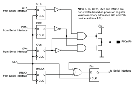 Figure 3. Simplified block diagram of PIO DS28CZ04 setting DS28CZ04 integrates multiple control functions and various features required by SFP on a single chip. The advantage of DS28CZ04 lies in its programmability, which is suitable for the application of cables of different lengths, and it needs to replace the components on the board (such as plug-in or 0Ω resistor). Except for cables, there is no need to replace the bill of materials for the entire copper cable series. In order to obtain proper circuit function, the memory of DS28CZ04 should be properly programmed. Please refer to the data specifications specified in the SFP MSA protocol or refer to the definition section of the digital diagnostic interface in the optical transceiver diagnostic monitoring port SFF-8472 specification. Special attention must be paid to the power-on default values of the four PIO ports. In this application, PIO0 is the input terminal, and PIO1 and PIO3 are the output terminals. All outputs are defined as open-drain outputs, because the inputs PE0, PE1, and OUTLEV of the MAX3982 have built-in pull-up resistors. Unless there are special circumstances, under normal circumstances, PIO1, PIO2, and PIO3 are in a high-level state after power-on, providing the strongest pre-emphasis output signal for 15 to 20 meters of cable. PIO input data does not need to be read inversely, and SFF mode is also one of the input options. If SFF mode is selected, the LOS signal of the MAX3748A can be read in through the DS28CZ04 memory address 6E (from address A2h) as real-time diagnosis. The SFF mode does not disable the output function of PIO1 and PIO1. The power-on state definition converts the data to the state specified by the data power-on default register. Tables 3 and 4 use color codes to indicate our selection.
 | | Value resulting from configuration / application requirements | | | Arbitrary assignment, "don't care" condition | |
Table 3. Power-on default values for PIO output status (lower half) and direction (higher half) | ADDR | b7 | b6 | b5 | b4 | b3 | b3 | b1 | b0 | Hex | | 76h | 0 | 0 | 0 | 1 | 1 | 1 | 1 | 1 | 1F | |
Table 4. Power-on default values for PIO read bit inversion (lower half bit) and output type (higher half bit) | ADDR | b7 | b6 | b5 | b4 | b3 | b3 | b1 | b0 | Hex | | 76h | 1 | 1 | 1 | 1 | 0 | 0 | 0 | 0 | F0 | |
The DS28CZ04 evaluation (EV) board needs to be demonstrated using a PC. For more information about the evaluation board, please refer to DS28CZ04EVKIT or contact the manufacturer. Conclusion For active copper cable SFP components, DS28CZ04 is a serial port control chip with high cost performance and flexible application. It not only meets the SFP / MSA specifications, but also meets the requirements of the optical transceiver SFF-8472 diagnostic monitoring interface.


 August 02, 2022

